Intel Shows Off Tile-Based Meteor Lake, Ponte Vecchio CPUs at Vision Event
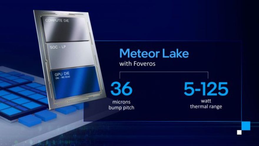
At this week’s Intel Vision event the company proudly displayed some of its next-gen silicon. Although its current and next generation CPUs feature a “hybrid” design, the company is moving to tile-based designs after that. Intel’s tiles are similar to chiplets, though there are some organizational differences in terms of what Intel intends to do with tiles versus how AMD has deployed chiplets. Intel’s next-generation Meteor Lake will still use hybrid cores, but the chip will field multiple tiles.
The CPUs Intel displayed are slated for 2023 and beyond, providing a rare glimpse into the company’s future products.
As a quick refresher, Intel is planning to release Raptor Lake this year as the successor to Alder Lake. It will be an optimized upgrade to the architecture using the same Intel 7 process. This is similar to Intel’s Tick-Tock strategy from yesteryear, where it introduces a CPU on a smaller node, then refines it. After Raptor Lake comes Meteor Lake, which will be a watershed product for Intel. It will be the company’s first tile-based CPU, utilizing both Intel and TSMC silicon. It’s remarkable in that it will combine three different manufacturing nodes on one package. It will feature four tiles, with the I/O and CPU tiles made on Intel 4 (formerly 7nm). The GPU will be a TSMC 3nm part with the SoC being a TSMC N4/N5 part, according to .

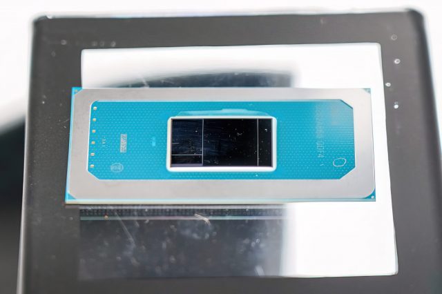
Intel’s Meteor Lake’s “standard” packaging. (Image: PC Watch)
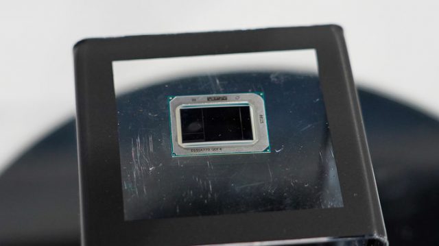
It’ll be the first client CPU to use and Embedded Multi-Die Interconnect Bridges (EMIB) to connect tiles both vertically and laterally. Intel displayed two versions of Meteor Lake: standard and high-density packaging. The standard packaging appears to be a mobile form factor, while the high-density looks more like a traditional desktop CPU. This is the main benefit to this approach; it can adjust an existing configuration for varying power requirements. Japanese site was on-hand for the event, and took plenty of photos.

Meteor Lake’s high-density packaging. (Image: PC Watch)
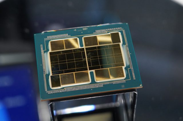
The company also showed off its big boy; Ponte Vecchio. This massive chip packs over 100 billion transistors and uses EMIB and Foveros to connect a whopping 47 tiles in a single package. Like Meteor Lake, tiles are connected both vertically and laterally. The chip was designed for the Department of Energy’s Aurora Exascale supercomputer, but will also be sold to customers working in the HPC and AI fields as well. This insanely complex chip will feature memory fabric capable of over 5TB/s of bandwidth.

Intel’s Ponte Vecchio chip represents the pinnacle of the company’s current engineering abilities. (Image: PC Watch)
Intel seems to be keeping pace with its lofty goal of advancing five nodes in four years. Those nodes are Intel 7, Intel 4, Intel 3, 20A, and 18A. This corresponds approximately to a refined Intel 10nm, Intel 7nm, and a future Intel 5nm under the old node naming regime. Showing off its chips like this is a way for it to reassure the public, and investors, that it’s still making progress. Intel’s CEO also recently flashed an 18A SRAM wafer at an investor meeting in February and said it’s currently .
Now Read: