IBM Announces Novel Advancement in 3D Wafer Stacking
At this point we’re all familiar with the global chip shortage. It’s affected every single industry in the world, it seems. Now IBM has come up with a new way to manufacture silicon wafers that it says could ease the strain a bit. It partnered with Tokyo Electron (TEL) on creating a new method for stacking silicon wafers vertically. Although IBM’s most advanced research node is currently 2nm, it doesn’t state which process it’s using for this technique. It only mentions it’s using it to stack 300mm (12-inch) wafers.
IBM’s claims it’s the first of its kind for a wafer of this size.

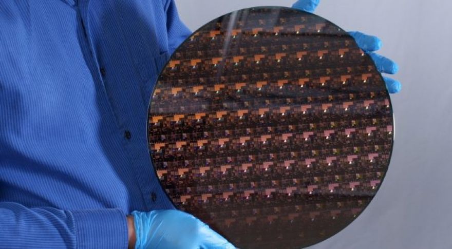
(Image: IBM)
IBM’s new process is essentially a novel way to join silicon wafers together. Traditional chip-stacking requires through-silicon vias (TSVs) between the layers. This allows electricity to flow upwards into the stack, and for both layers to work in tandem. This requires the backside of the layer to be thinned to reveal the TSVs for the other layer to connect to them. The layers in a stack are very thin, measuring less than 100 microns. Due to their fragility, they require a carrier wafer to support them.
Typically these carrier wafers are made of glass. The carrier wafer is bonded to the wafer to make sure it can go through production without being damaged. Once it’s finished production, the carrier is removed with a UV laser. In some cases a silicon carrier can be used too, but separating it from the layer requires a mechanical force. This can be dangerous for the integrity of the wafer it’s supposed to be protecting. This is where IBM’s new invention comes into play, as it’s figured out a way to debond two silicon wafers that’s transparent to silicon. It has achieved this by using an infrared laser to decouple the wafers.
This will allow two silicon wafers to be stacked without the use of glass carriers. Instead manufactures can just skip that step and go straight to silicon-to-silicon. IBM says in addition to simplifying the process by no longer requiring this extra step, there are other advantages as well. As an example it says it will help in eliminating tool compatibility and chucking issues, introduce fewer defects, and allow for inline testing of thinned wafers. These benefits will enable “advanced chiplet production” according to IBM. It also says its technology can scale very well.
IBM and TEL have been working on this technology since 2018, so it’s been in the hopper for a little while. This could be a crucial development for the industry given where things are headed in silicon fabrication. As node sizes shrink down to sub-2nm, packaging and stacking technologies will become a crucial advantage for companies looking to increase performance when “moving to a smaller node” is no longer an option.
Intel is already looking to begin advanced 3D stacking with , using its Foveros technology. AMD is way ahead of the game on that front, as mentioned previously. However, so far it’s only stacking L3 cache on its CPUs with Zen 3. However, there are rumors it will repeat that with Zen 4 as well with so-called Raphael-X products. It remains unclear if stacking will also be employed in its upcoming RDNA3 GPUs.
IBM says it’s built a beta tooling facility in Albany, NY to work on its new technology. In the future it will be expanding its work. Its goal is to eventually create a full 3D chip stack using this technology. The company says this advancement will help with supply chain issues, while also allowing for performance benefits too. “We hope our work will help cut down on the number of products needed in the semiconductor supply chain, while also helping drive processing power improvements for years to come,” it stated.
Now Read: